


Juniper CompatibleTAATAA compliant
QDD-400G-DR4-FLT
400G · QSFP-DD · 1310nmSMF · 500m · MPO
$2,400.00
QDD-400G-DR4-FLT, Juniper QDD-400G-DR4 Compatible 400GBase-DR4 QSFP56-DD 1310nm 500m DOM MPO SMF TAA Optical Transceiver Module Proudly Owned and Operated in the U.S.A. Since 2003
Need a larger quantity? Request a quote
Questions? Call (888) 874-7574
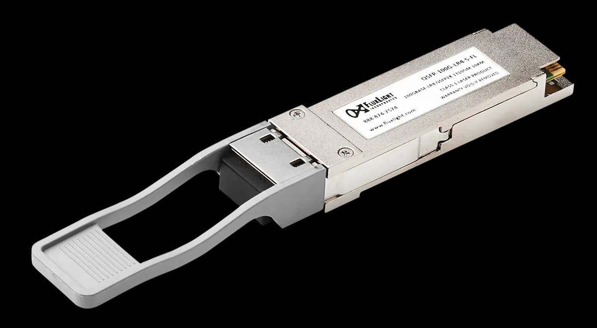
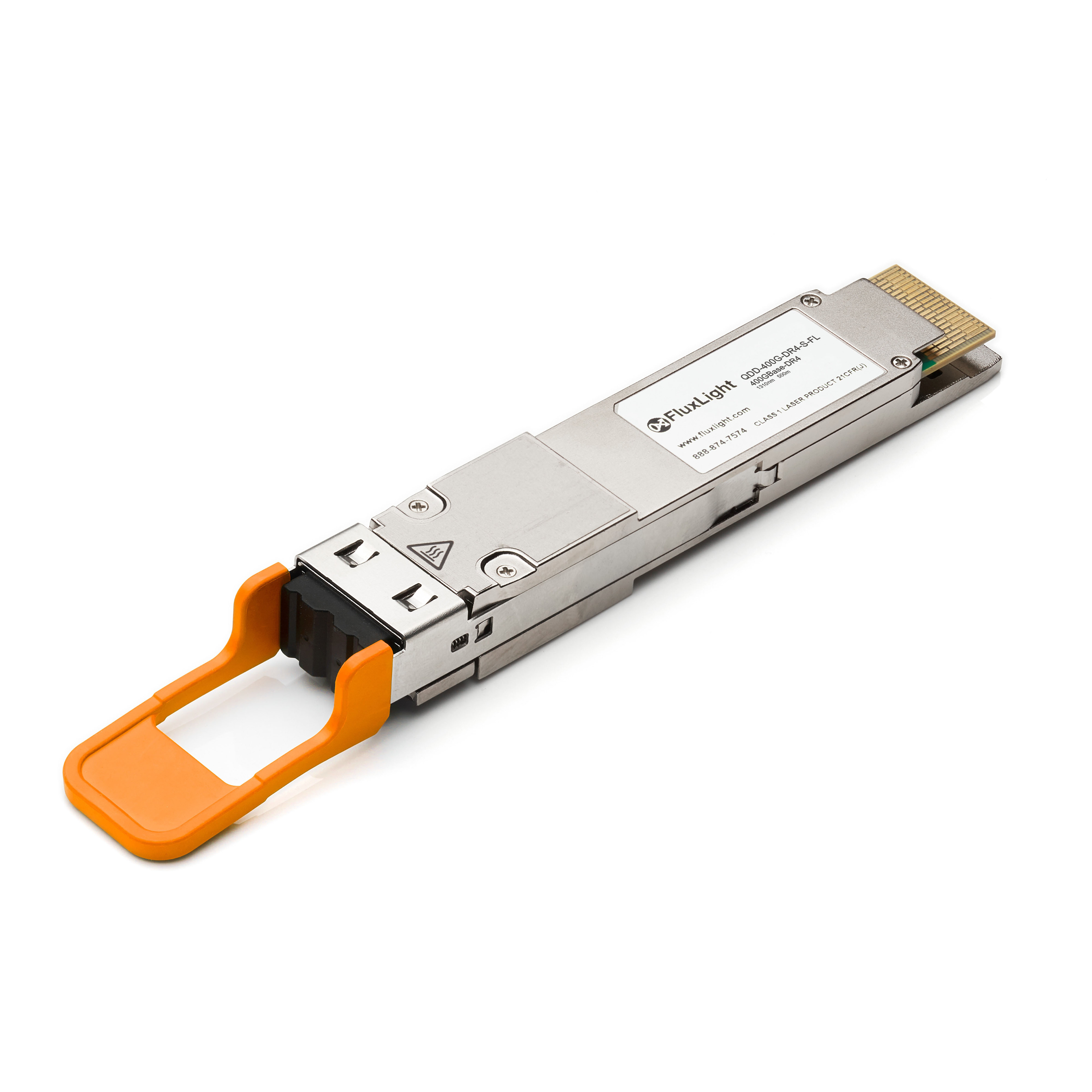
The QDD-400G-DR4-FL is a 400Gb/s Quad Small Form Factor Pluggable-double density (QSFP56-DD) optical module designed for 500m optical communication applications. The module converts 8 channels of 50Gb/s (PAM4) electrical input data to 4 channels of parallel optical signals, each capable of 100Gb/s operation for an aggregate data rate of 400Gb/s. Reversely, on the receiver side, the module converts 4 channels of parallel optical signals of 100Gb/s each channel for an aggregate data rate of 400Gb/s into 8 channels of 50Gb/s (PAM4) electrical output data.
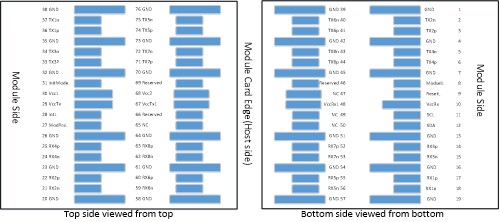
| Pin | Logic | Symbol | Description |
|---|---|---|---|
| 1 | GND | Ground | |
| 2 | CML | Tx2n | Transmitter Inverted Data Input |
| 3 | CML | Tx2p | Transmitter Non-Inverted Data Input |
| 4 | GND | Ground | |
| 5 | CML | Tx4n | Transmitter Inverted Data Input |
| 6 | CML | Tx4p | Transmitter Non-Inverted Data Input |
| 7 | GND | Ground | |
| 8 | LVTTL | ModSelL | Module Select |
| 9 | LVTTL | ResetL | Module Reset |
| 10 | VccRx | Receiver +3.3V DC Power Supply | |
| 11 | LVCMOS | SCL | 2-wire serial interface clock |
| 12 | LVCMOS | SDA | 2-wire serial interface data |
| 13 | GND | Ground | |
| 14 | CML | Rx3p | Receiver Non-Inverted Data Output |
| 15 | CML | Rx3n | Receiver Inverted Data Output |
| 16 | GND | Ground | |
| 17 | CML | Rx1p | Receiver Non-Inverted Data Output |
| 18 | CML | Rx1n | Receiver Inverted Data Output |
| 19 | GND | Ground | |
| 20 | GND | Ground | |
| 21 | CML | Rx2n | Receiver Inverted Data Output |
| 22 | CML | Rx2p | Receiver Non-Inverted Data Output |
| 23 | GND | Ground | |
| 24 | CML | Rx4n | Receiver Inverted Data Output |
| 25 | CML | Rx4p | Receiver Non-Inverted Data Output |
| 26 | GND | Ground | |
| 27 | LVTTL | ModPrsL | Module Present |
| 28 | LVTTL | IntL | Interrupt |
| 29 | VccTx | Transmitter +3.3V DC Power Supply | |
| 30 | Vcc1 | +3.3V DC Power Supply | |
| 31 | LVTTL | InitMode | Initialization Mode (called LPMode in legacy QSFP applications) |
| 32 | GND | Ground | |
| 33 | CML | Tx3p | Transmitter Non-Inverted Data Input |
| 34 | CML | Tx3n | Transmitter Inverted Data Input |
| 35 | GND | Ground | |
| 36 | CML | Tx1p | Transmitter Non-Inverted Data Input |
| 37 | CML | Tx1n | Transmitter Inverted Data Input |
| 38 | GND | Ground | |
| 39 | GND | Ground | |
| 40 | CML | Tx6n | Transmitter Inverted Data Input |
| 41 | CML | Tx6p | Transmitter Non-Inverted Data Input |
| 42 | GND | Ground | |
| 43 | CML | Tx8n | Transmitter Inverted Data Input |
| 44 | CML | Tx8p | Transmitter Non-Inverted Data Input |
| 45 | GND | Ground | |
| 46 | Reserved | For future use | |
| 47 | VS1 | Module Vendor Specific 1 | |
| 48 | VccRx1 | +3.3V DC Power Supply | |
| 49 | VS2 | Module Vendor Specific 2 | |
| 50 | VS3 | Module Vendor Specific 3 | |
| 51 | GND | Ground | |
| 52 | CML | Rx7p | Receiver Non-Inverted Data Output |
| 53 | CML | Rx7n | Receiver Inverted Data Output |
| 54 | GND | Ground | |
| 55 | CML | Rx5p | Receiver Non-Inverted Data Output |
| 56 | CML | Rx5n | Receiver Inverted Data Output |
| 57 | GND | Ground | |
| 58 | GND | Ground | |
| 59 | CML | Rx6n | Receiver Inverted Data Output |
| 60 | CML | Rx6p | Receiver Non-Inverted Data Output |
| 61 | GND | Ground | |
| 62 | CML | Rx8n | Receiver Inverted Data Output |
| 63 | CML | Rx8p | Receiver Non-Inverted Data Output |
| 64 | GND | Ground | |
| 65 | NC | No Connect | |
| 66 | Reserved | For future use | |
| 67 | VccTx1 | +3.3V DC Power Supply | |
| 68 | Vcc2 | +3.3V DC Power Supply | |
| 69 | Reserved | For future use | |
| 70 | GND | Ground | |
| 71 | CML | Tx7p | Transmitter Non-Inverted Data Input |
| 72 | CML | Tx7n | Transmitter Inverted Data Input |
| 73 | GND | Ground | |
| 74 | CML | Tx5p | Transmitter Non-Inverted Data Input |
| 75 | CML | Tx5n | Transmitter Inverted Data Input |
| 76 | GND | Ground |
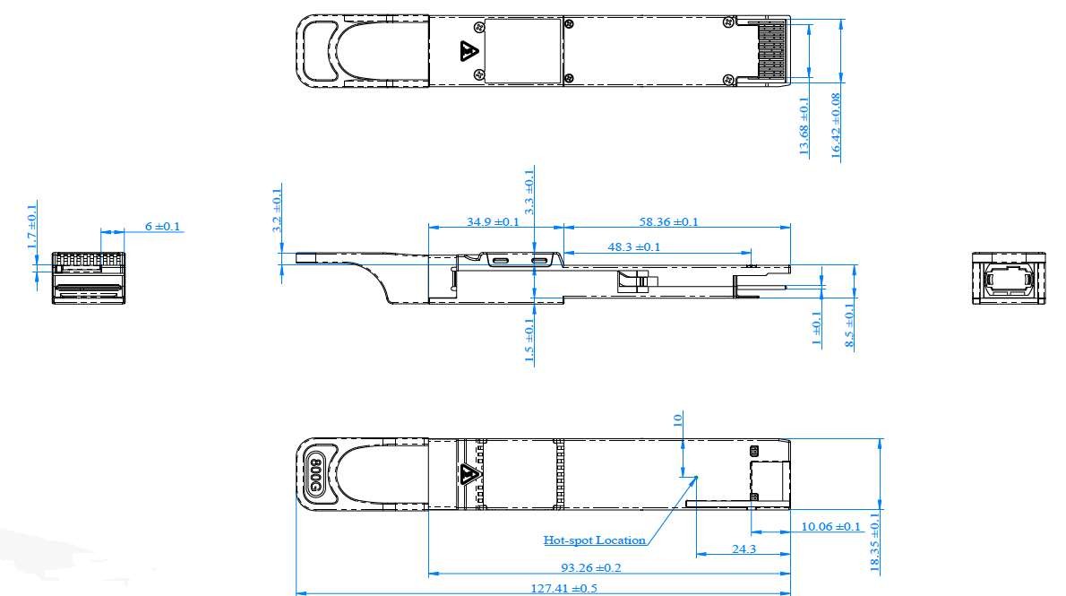
The optical port is an MPO-12 APC receptacle carrying 4 transmit and 4 receive single-mode fibers. Proper alignment is ensured by the guide pins inside the receptacle; the cable should not be twisted, to keep channel-to-channel alignment.
Operation in excess of any individual absolute maximum rating may cause permanent damage to the module.
| Parameter | Symbol | Min | Max | Unit |
|---|---|---|---|---|
| Storage Temperature | TS | -40 | 85 | °C |
| Operating Case Temperature | TOP | 0 | 70 | °C |
| Power Supply Voltage | VCC | -0.5 | 3.6 | V |
| Relative Humidity (non-condensation) | RH | 0 | 85 | % |
| Damage Threshold, each Lane | THd | 5 | dBm |
| Parameter | Symbol | Min | Typical | Max | Unit | Notes |
|---|---|---|---|---|---|---|
| Operating Case Temperature | TOP | 0 | 70 | °C | ||
| Power Supply Voltage | VCC | 3.135 | 3.3 | 3.465 | V | |
| Data Rate, each Lane | 26.5625 | GBd | PAM4 | |||
| Data Rate Accuracy | -100 | 100 | ppm | |||
| Pre-FEC Bit Error Ratio | 2.4×10⁻⁴ | |||||
| Post-FEC Bit Error Ratio | 1×10⁻¹² | 1 | ||||
| Link Distance (SMF) | D | 2 | 500 | m | 2 |
The following electrical characteristics are defined over the Recommended Operating Environment unless otherwise specified.
| Parameter | Test Point | Min | Typical | Max | Unit | Notes |
|---|---|---|---|---|---|---|
| Power Consumption | 12 | W | ||||
| Supply Current | Icc | 3.64 | A | |||
| Transmitter (each Lane) | ||||||
| Signaling Rate, each Lane | TP1 | 26.5625 ± 100 ppm | GBd | |||
| Differential pk-pk Input Voltage Tolerance | TP1a | 900 | mVpp | 1 | ||
| Differential Termination Mismatch | TP1 | 10 | % | |||
| Differential Input Return Loss | TP1 | IEEE 802.3-2015 Equation (83E-5) | dB | |||
| Differential to Common Mode Input Return Loss | TP1 | IEEE 802.3-2015 Equation (83E-6) | dB | |||
| Module Stressed Input Test | TP1a | See IEEE 802.3bs 120E.3.4.1 | 2 | |||
| Single-ended Voltage Tolerance Range | TP1a | -0.4 | 3.3 | V | ||
| DC Common Mode Input Voltage | TP1 | -350 | 2850 | mV | 3 | |
| Receiver (each Lane) | ||||||
| Signaling Rate, each Lane | TP4 | 26.5625 ± 100 ppm | GBd | |||
| Differential Peak-to-Peak Output Voltage | TP4 | 900 | mVpp | |||
| AC Common Mode Output Voltage, RMS | TP4 | 17.5 | mV | |||
| Differential Termination Mismatch | TP4 | 10 | % | |||
| Differential Output Return Loss | TP4 | IEEE 802.3-2015 Equation (83E-2) | dB | |||
| Common to Differential Mode Conversion Return Loss | TP4 | IEEE 802.3-2015 Equation (83E-3) | dB | |||
| Transition Time, 20% to 80% | TP4 | 9.5 | ps | |||
| Near-end Eye Symmetry Mask Width (ESMW) | TP4 | 0.265 | UI | |||
| Near-end Eye Height, Differential | TP4 | 70 | mV | |||
| Far-end Eye Symmetry Mask Width (ESMW) | TP4 | 0.2 | UI | |||
| Far-end Eye Height, Differential | TP4 | 30 | mV | |||
| Far-end Pre-cursor ISI Ratio | TP4 | -4.5 | 2.5 | % | ||
| Common Mode Output Voltage (Vcm) | TP4 | -350 | 2850 | mV | 3 | |
The following optical characteristics are defined over the Recommended Operating Environment unless otherwise specified.
| Parameter | Symbol | Min | Typical | Max | Unit | Notes |
|---|---|---|---|---|---|---|
| Center Wavelength | λc | 1304.5 | 1310 | 1317.5 | nm | |
| Transmitter | ||||||
| Data Rate, each Lane | 53.125 ± 100 ppm | GBd | ||||
| Modulation Format | PAM4 | |||||
| Side-mode Suppression Ratio | SMSR | 30 | dB | |||
| Average Launch Power, each Lane | PAVG | -2.9 | 4 | dBm | 1 | |
| Outer Optical Modulation Amplitude (OMAouter), each Lane | POMA | -0.8 | 4.2 | dBm | 2 | |
| Launch Power in OMAouter minus TDECQ, each Lane, for ER ≥ 5 dB | -2.2 | dBm | ||||
| Launch Power in OMAouter minus TDECQ, each Lane, for ER < 5 dB | -1.9 | dBm | ||||
| Transmitter and Dispersion Eye Closure for PAM4 (TDECQ), each Lane | TDECQ | 3.4 | dB | |||
| TDECQ − 10·log10(Ceq), each Lane | 3.4 | dB | 3 | |||
| Extinction Ratio | ER | 3.5 | dB | |||
| RIN21.4OMA | RIN | -136 | dB/Hz | |||
| Optical Return Loss Tolerance | TOL | 21.4 | dB | |||
| Transmitter Reflectance | TR | -26 | dB | |||
| Transmitter Transition Time | 17 | ps | ||||
| Average Launch Power of OFF Transmitter, each Lane | Poff | -15 | dBm | |||
| Receiver | ||||||
| Data Rate, each Lane | 53.125 ± 100 ppm | GBd | ||||
| Modulation Format | PAM4 | |||||
| Damage Threshold, each Lane | THd | 5 | dBm | 5 | ||
| Average Receive Power, each Lane | -5.9 | 4 | dBm | 4 | ||
| Receive Power (OMAouter), each Lane | 4.2 | dBm | ||||
| Receiver Sensitivity (OMAouter), each Lane | SEN | max(−3.9, SECQ − 5.3) | dBm | 6 | ||
| Stressed Receiver Sensitivity (OMAouter), each Lane | SRS | -1.9 | dBm | 7 | ||
| Receiver Reflectance | RR | -26 | dB | |||
| LOS Assert | LOSA | -15 | dBm | |||
| LOS De-assert | LOSD | -8.9 | dBm | |||
| LOS Hysteresis | LOSH | 0.5 | dB | |||
| Stressed Conditions for Stressed Receiver Sensitivity | 8 | |||||
| Stressed Eye Closure for PAM4 (SECQ), Lane under Test | 3.4 | dB | ||||
| SECQ − 10·log10(Ceq), Lane under Test | 3.4 | dB | ||||
| OMAouter of each Aggressor Lane | 4.2 | dBm | ||||
The following digital diagnostic characteristics are defined over the normal operating conditions unless otherwise specified.
| Parameter | Symbol | Min | Max | Unit | Notes |
|---|---|---|---|---|---|
| Temperature monitor absolute error | DMI_Temp | -3 | 3 | °C | Over operating temperature range |
| Supply voltage monitor absolute error | DMI_VCC | -0.1 | 0.1 | V | Over full operating range |
| Channel RX power monitor absolute error | DMI_RX_Ch | -2 | 2 | dB | 1 |
| Channel bias current monitor absolute error | DMI_Ibias_Ch | -10 | 10 | % | |
| Channel TX power monitor absolute error | DMI_TX_Ch | -2 | 2 | dB | 1 |
This transceiver is specified as ESD threshold 1kV for high-speed data pins and 2kV for all other electrical input pins, tested per MIL-STD-883, Method 3015.4 /JESD22-A114-A (HBM). However, normal ESD precautions are still required during the handling of this module. This transceiver is shipped in ESD protective packaging. It should be removed from the packaging and handled only in an ESD protected environment.
This is a Class 1 Laser Product according to EN 60825-1:2014. This product complies with 21 CFR 1040.10 and 1040.11 except for deviations pursuant to Laser Notice No. 50, dated (June 24, 2007).
Caution: Use of controls or adjustments or performance of procedures other than those specified herein may result in hazardous radiation exposure.
FluxLight is fully committed to environment protection and sustainable development and has set in place a comprehensive program for removing polluting and hazardous substances from all of its products. The relevant evidence of RoHS compliance is held as part of our controlled documentation for each of our compliant products. RoHS compliance parts are available to order, please refer to the ordering information section for further details.
The following is a list of Finisar Corporation patents Fluxlight has licensed. This licensure recognizes and compensates Finisar for their intellectual property. The QDD-400G-DR4-FL, like all Fluxlight optical transceivers, is covered by this license agreement. Therefore, Fluxlight customers can rest assured that all products purchased are fully licensed, and our customers are under no potential liability that may ensue from the use of unlicensed optical transceiver products.
U.S. Patent Numbers: 7,184,668 (System and method of protecting eye safety during operation of a fiber optic transceiver), 7,079,775 (Integrated memory mapped controller circuit for fiber optics transceiver), 6,957,021 (Optical transceiver with memory mapped locations), 7,058,310 (System and method for protecting eye safety during operation of a fiber optic transceiver), 6,952,531 (System and method for protecting eye safety during operation of a fiber optic transceiver), 7,162,160 (System and method for protecting eye safety during operation of a fiber optic transceiver), 7,050,720 (Integrated memory mapped controller circuit for fiber optics transceiver)
Original Equipment Manufacturer (OEM) names may be registered trademarks of the respective OEM, and the OEM has neither authorized nor sponsored the use of its trademark or trade name. All OEM names are used for cross reference/comparative purposes only.
This part is covered by our Limited Lifetime Warranty, a 10-year serviceable lifetime, and our 30-Day Money-Back Guarantee. Read the full warranty and return terms.
No reviews yet. If you have used this part, yours would be the first.
Get compatible transceivers and cables shipped fast, with expert support when you need it.


150 in stock
Order by 3 PM CT for same-day shipping


400G · QSFP-DD · 1310nmSMF · 500m · MPO

400G · QSFP-DD · 1310nmSMF · 500m · MPO
400G · QSFP-DD · 1310nmSMF · 500m · MPO

400G · QSFP-DD · 1310nmSMF · 500m · MPO