

Cisco Compatible
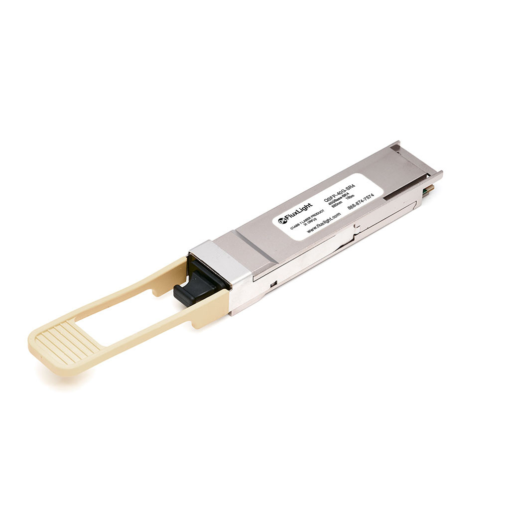
QSFP-40G-SR4-FL
40G · QSFP+ · 850nmMMF · 150m · MPO
$42.99
QSFP-40G-SR4-FL, Cisco QSFP-40G-SR4 Compatible 40GBASE-SR4 QSFP+ Transceiver, 850nm, 150m, MMF, MPO-12 Proudly Owned and Operated in the U.S.A. Since 2003
Need a larger quantity? Request a quote
Questions? Call (888) 874-7574
The FluxLight QSFP-40G-SR4-S-FL is a Cisco QSFP-40G-SR4-S compatible 40GBASE-SR4 QSFP+ transceiver for 40 Gigabit Ethernet over multimode fiber up to 100 m on OM3 and 150 m on OM4. It transmits at 850 nm, uses an MPO-12 connector and supports digital diagnostics (DOM).
The QSFP-40G-SR4-S-FL is coded for Cisco and works in the Cisco ports that take the QSFP-40G-SR4-S, including Nexus 3000, Nexus 9100 / 9200 / 9300, ASR 9000 and NCS 5500. Platform Support lists every supported model across 32 platform families.
It meets IEEE 802.3ba 40GBASE-SR4, so it links to any 40GBASE-SR4 optic at the far end, whatever its brand. It follows the QSFP+ MSA and reports temperature, supply voltage, laser bias and optical power through SFF-8436 diagnostics. It uses a VCSEL array and a PIN photodiode array, draws at most 1.5 W and is rated for a case temperature of 0 to 70 °C (commercial grade).
FluxLight guarantees it is compatible with Cisco and covers it with a 10-year warranty. The TAA-compliant version is QSFP-40G-SR4-S-FLT.
The operation in excess of any absolute maximum ratings might cause permanent damage to this module.
| Parameter | Symbol | Min | Max | Unit |
|---|---|---|---|---|
| Storage Temperature | TS | -40 | 85 | °C |
| Power Supply Voltage | VCC | 0 | 3.6 | V |
| Relative Humidity | RH | 0 | 85 | % |
| Parameter | Symbol | Min | Typical | Max | Unit | Notes |
|---|---|---|---|---|---|---|
| Operating Case Temperature | TOP | 0 | 70 | °C | ||
| Supply Voltage | VCC | 3.135 | 3.3 | 3.465 | V | |
| Data Rate (Each Lane) | DR | 10.3125 | Gb/s | |||
| Power Consumption | PC | 1.5 | W | |||
| Link Distance with OM3 | D | 100 | m | Per IEEE 802.3ba 40GBASE-SR4 | ||
| Link Distance with OM4 | D | 150 | m | Per IEEE 802.3ba 40GBASE-SR4 |
The following electrical characteristics are defined over the Recommended Operating Environment unless otherwise specified.
| Parameter | Symbol | Min | Typical | Max | Unit |
|---|---|---|---|---|---|
| Differential Data Input Swing | VIN | 100 | 900 | mV | |
| Input Differential Impedance | Zin | 100 | Ω | ||
| Transmitter Disable Voltage | VD | 2.0 | Vcc | V | |
| Transmitter Enable Voltage | VEN | 0 | 0.8 | V | |
| Differential Data Output Swing | VOUT | 300 | 600 | 900 | mV |
| Output Differential Impedance | Zout | 100 | Ω | ||
| LOS Assert Voltage | VLOSA | 2.0 | Vcc | V | |
| LOS De-assert Voltage | VLOSD | 0 | 0.8 | V |
| Parameter | Symbol | Min | Typical | Max | Unit | Notes |
|---|---|---|---|---|---|---|
| Transmitter | ||||||
| Average Output Power, each lane | POUT | -7.6 | 2.4 | dBm | ||
| Optical Modulation Amplitude, each lane | OMA | -5.6 | 3 | dBm | ||
| Extinction Ratio | ER | 3 | dB | |||
| Average Output Power (Laser Off) | POFF | -30 | dBm | |||
| Center Wavelength | λ | 840 | 850 | 860 | nm | |
| RMS Spectral Width | σλ | 0.65 | nm | Per IEEE 802.3ba 40GBASE-SR4 | ||
| Receiver | ||||||
| Average Receive Power, each lane | Pin | -9.5 | 2.4 | dBm | ||
| Unstressed Receiver Sensitivity (OMA), each lane | Sen | -9.5 | dBm | Measured at 10.3125 Gb/s, PRBS 2³¹−1 | ||
| Stressed Receiver Sensitivity (OMA), each lane | SRS | -5.4 | dBm | Per IEEE 802.3ba 40GBASE-SR4 | ||
| Receiver Damage Threshold, per Lane | PRdmg | 3.4 | dBm | |||
| Center Wavelength | λ | 840 | 850 | 860 | nm | |
| LOS Assert | LOSA | -30 | dBm | |||
| LOS De-Assert | LOSD | -12 | dBm | |||
| LOS Hysteresis | LOSH | 0.5 | 6 | dB | ||
The following digital diagnostic characteristics are defined over the normal operating conditions unless otherwise specified.
| Parameter | Symbol | Min | Max | Unit |
|---|---|---|---|---|
| Temperature monitor absolute error | DMI_Temp | -5 | 5 | °C |
| Supply voltage monitor absolute error | DMI_VCC | -0.1 | 0.1 | V |
| Channel RX power monitor absolute error | DMI_RX_Ch | -3 | 3 | dB |
| Channel bias current monitor absolute error | DMI_Ibias_Ch | -10% | 10% | mA |
| Channel TX power monitor absolute error | DMI_TX_Ch | -3 | 3 | dB |
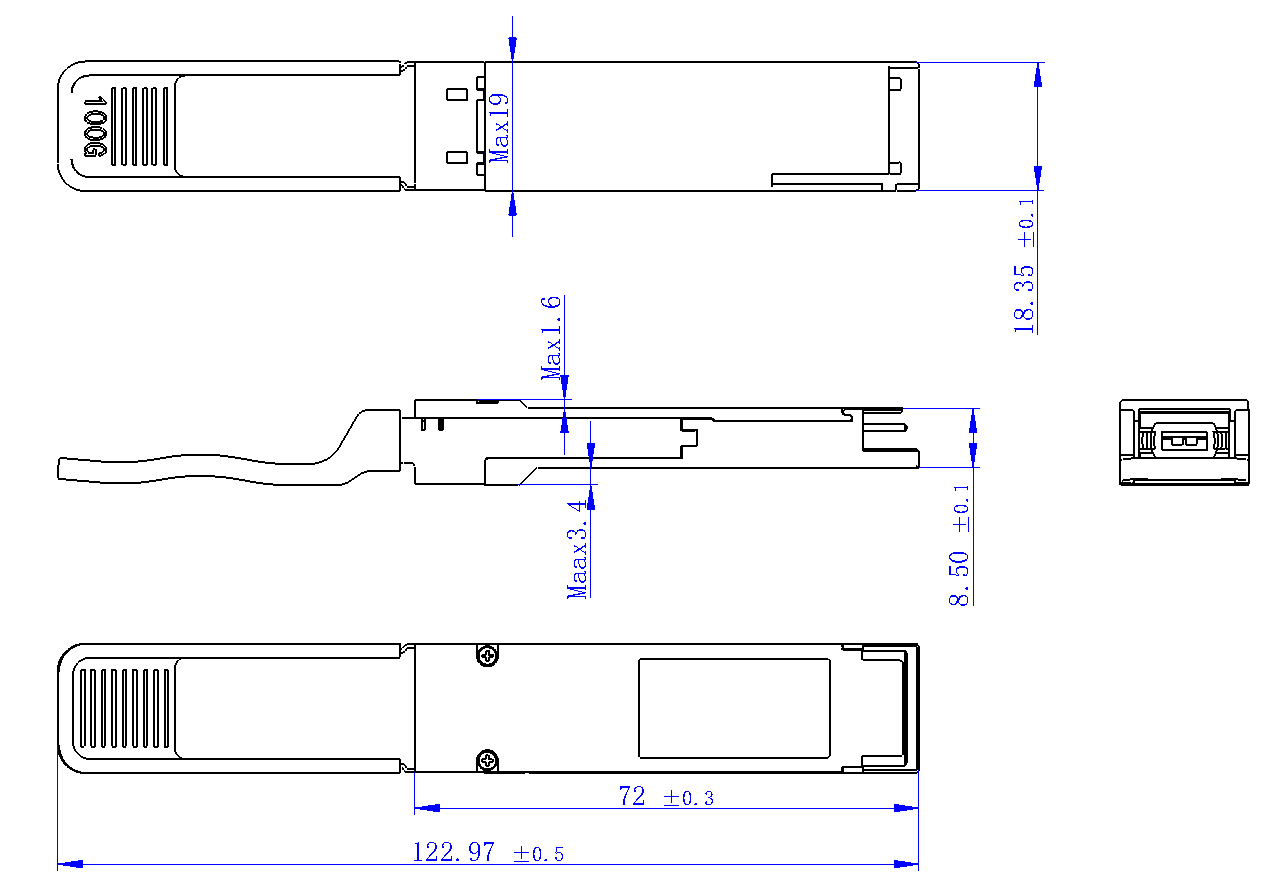
Units: mm
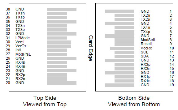
| Pin | Logic | Symbol | Description | Plug Sequence |
|---|---|---|---|---|
| 1 | GND | Ground | 1 | |
| 2 | CML-I | Tx2n | Transmitter Inverted Data Input | 3 |
| 3 | CML-I | Tx2p | Transmitter Non-Inverted Data Input | 3 |
| 4 | GND | Ground | 1 | |
| 5 | CML-I | Tx4n | Transmitter Inverted Data Input | 3 |
| 6 | CML-I | Tx4p | Transmitter Non-Inverted Data Input | 3 |
| 7 | GND | Ground | 1 | |
| 8 | LVTTL-I | ModSelL | Module Select | 3 |
| 9 | LVTTL-I | ResetL | Module Reset | 3 |
| 10 | VccRx | +3.3V Power Supply Receiver | 2 | |
| 11 | LVCMOS-I/O | SCL | 2-Wire Serial Interface Clock | 3 |
| 12 | LVCMOS-I/O | SDA | 2-Wire Serial Interface Data | 3 |
| 13 | GND | Ground | 1 | |
| 14 | CML-O | Rx3p | Receiver Non-Inverted Data Output | 3 |
| 15 | CML-O | Rx3n | Receiver Inverted Data Output | 3 |
| 16 | GND | Ground | 1 | |
| 17 | CML-O | Rx1p | Receiver Non-Inverted Data Output | 3 |
| 18 | CML-O | Rx1n | Receiver Inverted Data Output | 3 |
| 19 | GND | Ground | 1 | |
| 20 | GND | Ground | 1 | |
| 21 | CML-O | Rx2n | Receiver Inverted Data Output | 3 |
| 22 | CML-O | Rx2p | Receiver Non-Inverted Data Output | 3 |
| 23 | GND | Ground | 1 | |
| 24 | CML-O | Rx4n | Receiver Inverted Data Output | 3 |
| 25 | CML-O | Rx4p | Receiver Non-Inverted Data Output | 3 |
| 26 | GND | Ground | 1 | |
| 27 | LVTTL-O | ModPrsL | Module Present | 3 |
| 28 | LVTTL-O | IntL | Interrupt | 3 |
| 29 | VccTx | +3.3V Power Supply Transmitter | 2 | |
| 30 | Vcc1 | +3.3V Power Supply | 2 | |
| 31 | LVTTL-I | LPMode | Low Power Mode | 3 |
| 32 | GND | Ground | 1 | |
| 33 | CML-I | Tx3p | Transmitter Non-Inverted Data Input | 3 |
| 34 | CML-I | Tx3n | Transmitter Inverted Data Input | 3 |
| 35 | GND | Ground | 1 | |
| 36 | CML-I | Tx1p | Transmitter Non-Inverted Data Input | 3 |
| 37 | CML-I | Tx1n | Transmitter Inverted Data Input | 3 |
| 38 | GND | Ground | 1 |
This transceiver is specified as an ESD threshold of 1kV for the high-speed data pins and 2kV for all other electrical input pins, tested per MIL-STD-883, Method 3015.4 / JESD22-A114-A (Human Body Model). However, normal ESD precautions are still required during the handling of this module. This transceiver is shipped in ESD-protective packaging. It should be removed from the packaging and handled only in an ESD-protected environment.
This is a Class 1 Laser Product according to IEC 60825-1:2007. This product complies with 21 CFR 1040.10 and 1040.11 except for deviations pursuant to Laser Notice No. 50, dated (June 24, 2007).
This part is covered by our Limited Lifetime Warranty, a 10-year serviceable lifetime, and our 30-Day Money-Back Guarantee. Read the full warranty and return terms.
No reviews yet. If you have used this part, yours would be the first.
Get compatible transceivers and cables shipped fast, with expert support when you need it.


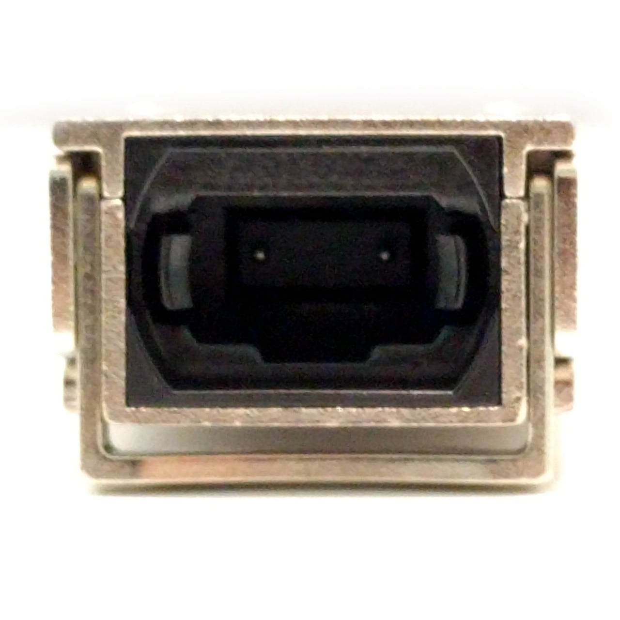
495 in stock
Order by 3 PM CT for same-day shipping


40G · QSFP+ · 850nmMMF · 150m · MPO

40G · QSFP+ · 850nmMMF · 150m · MPO
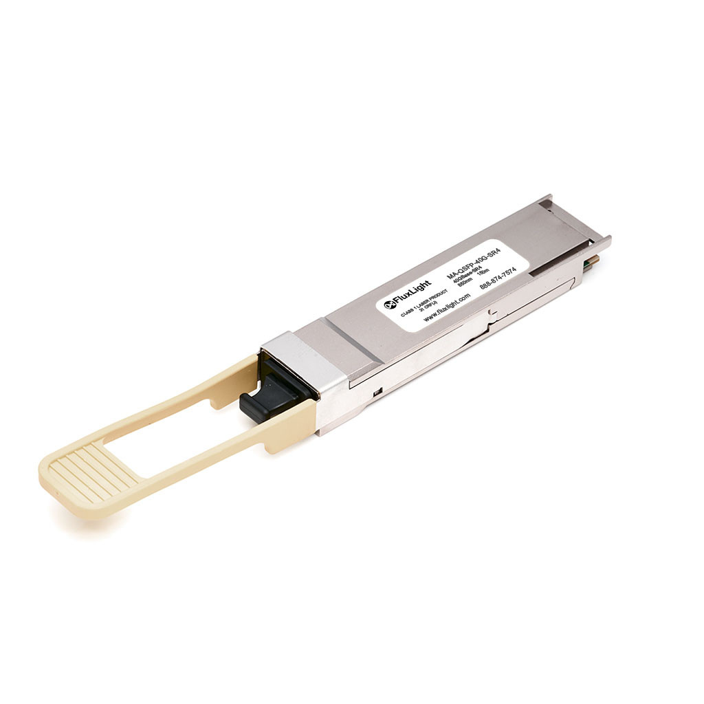
40G · QSFP+ · 850nmMMF · 150m · MPO

40G · QSFP+ · 850nmMMF · 150m · MPO